技術摘要: 技術摘要: |
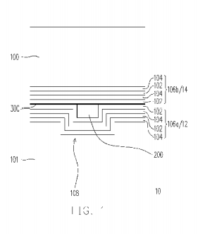
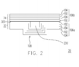
A semiconductor hollow optical waveguide (SHOW-ODR) device. The semiconductor hollow optical waveguide device comprises a bottom substrate having a trench within, a first omni-directional reflector conformal located on the bottom substrate, and a top substrate having a second omni-directional reflector and located on the bottom substrate with the second omni-directional reflector in contact with the first omni-directional reflector. In addition, a portion of the first omni-directional reflector in the trench and a portion of the second omni-directional reflector over the trench together form an air channel.
|
| 解決的問題或達成的功效: |
The present invention relates to a type of semiconductor waveguide device. In particular, the present invention relates to a hollow semiconductor optical waveguide device and a method of manufacturing the same.
|
| 應用領域: |
|
| 適用產品: |
|
| IPC: |
G02B6/10
|
| Claim 1: |
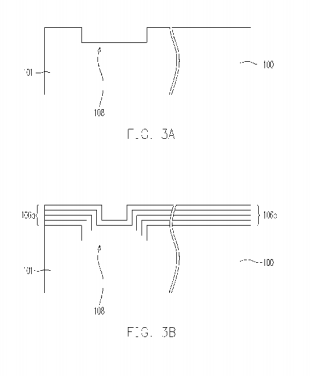
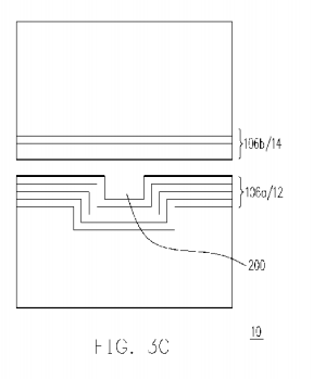
1. A method of manufacturing a SHOW-ODR device, comprising:
providing a top substrate and a bottom substrate;
forming a trench on the bottom substrate;
forming thin layers of stacking a plurality of alternating layers of a first material layer and a second material layer on both the top substrate and the bottom substrate, wherein the alternating layers of the first material layer and the second material layer on the bottom substrate and the top substrate are a first multi-layered structure and a second multi-layered structure respectively; and
performing a wafer bonding to join the bottom substrate and the top substrate, wherein the first multi-layered structure is directly in contact with the second multi-layered structure, and the wafer bonding includes anodic bonding, fusion bonding, high vacuum bonding, or chemical bonding.
|
| 相關圖片: |
|
|
| 聯繫方式 |
|
| |